
Binning is the process of combining charge from
adjacent pixels in a CCD during readout. This process is performed prior to
digitization in the on-chip circuitry of the CCD by specialized control of the
serial and parallel registers. The two primary benefits of binning are improved
signal-to-noise ratio (SNR) and the ability to increase frame
rate, albeit at the expense of reduced spatial resolution.
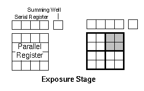
To understand the process, consider the example of 2 x 2 binning
shown below. As in normal operation, charge integrates in individual
pixels while the CCD is exposed to light. During the parallel
readout, the charge from two rows of pixels, rather than a single
row, is shifted into the serial register. Next, charge is shifted
from the serial register, two pixels at a time, into the summing
well. It then goes to the output amplifier where it is converted
to a voltage before being transferred off-chip for further amplification
and digitization. This procedure is iterated until the entire
array has been read out. The result is that each readout event
from the summing well contains the collected charge from four
pixels on the CCD. It should be noted that our camera have the
ability to perform binning into any arbitrary M x N binned pixels
(super-pixels) through simple software control.
Since both the serial register and summing well accumulate charge
from multiple pixels during binning, they must have sufficient
capacity to prevent saturation. In HCCDs, the serial register
typically has a charge capacity double that of the parallel registers,
and the summing well double that of the serial register. However,
the specifications of the particular CCD being used should be
noted and understood before using the binning technique. This
is especially true when working at high-illumination levels where
saturation could lead to erroneous data collection.
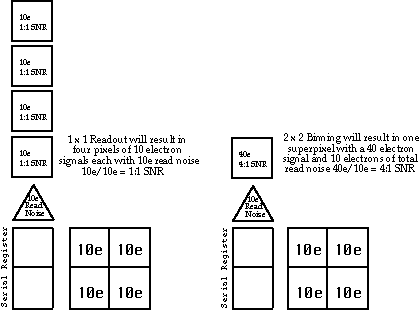
The primary benefit of binning is higher SNR due to reduced read noise contributions. CCD read noise is added during each readout event and in normal operation, read noise will be added to each pixel. However, in binning mode read noise is added to each super-pixel which has the combined signal from multiple pixels. In the ideal case, this produces a SNR improvement equal to the binning factors (4x in the above example). The figure below shows the effect of 2 x 2 binning for a four pixel region. This example assumes that 10 photoelectrons have been collected in each pixel and the read noise is 10 electrons. If this region is read out in normal mode the SNR will be 1:1, and the signal will be lost in the noise. However, with 2 x 2 binning, the SNR becomes 4:1 which is sufficient to observe this weak signal.
Unlike read noise, dark current noise is not reduced by binning since each pixel will contribute dark current noise to the super-pixel. To ensure that dark current noise does not lower SNR during binning, it is essential that the CCD be cooled sufficiently to reduce the dark current noise to a negligible level relative to the read noise.
One of the most common applications of binning is spectroscopy. In spectroscopic CCD systems, the dispersed slit images lie along the CCD columns (perpendicular to the serial register) and the resulting images are then binned along the columns. Binning thus provides marked increases in SNR without any loss of spectral resolution. Spatial resolution is lost along the slit axis but this typically is not a concern. Another use of binning is to increase frame rate. Since the slowest step in the readout sequence is the digitization of a given pixel, binning can be used to increase the effective total frame rate of a given system. Thus, highly binned low-resolution images can be obtained when high speed is required (such as in focusing) and full-frame high-resolution images can be obtained when the ultimate resolution is required.